Thin film deposition, vacuum furnace and semiconductor applications utilize SHI’s Cryopumps and select Cryocoolers.

The number of technologies that make up the “High Technology” sector and utilize thin film deposition are enormous in number:
- Flat panel displays include televisions, computer screens, tablets, laptops, smart phones or any device requiring a high resolution display. Picture tubes are in our distant memory as we have seen televisions evolve. LCD continues to remain the dominant technology in the market, while up and coming technologies include OLED, as well as next gen QD-OLED, QNED, and MicroLED.
- Solar energy is a dream of many wishing to see the status quo migrate to more energy independence, with less impact on the environment. Advances in thin film technology allow for more efficient production of the solar cells, ultimately leading to a more robust energy converting source.
- General coating applications are used in the creation of many common products that are coated under vacuum, including sunglasses, automobile parts, glass and many more.
Many of these high technology products are manufactured using some level of high vacuum, which typically requires cryopumps, water traps or cryocoolers to improve the quality of the end product. Cryopump systems trap contaminates from the chamber, ensuring a high level of purity before proceeding with the process steps. Without this critical step, high purity levels would not be achievable otherwise, and many technologies used today would not be possible.
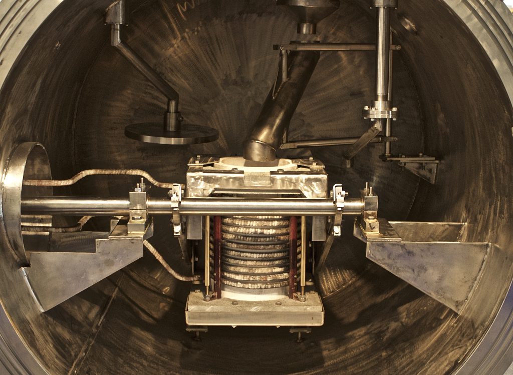
The sealed chamber of a vacuum furnace utilizes vacuum pumps to remove air and gas from the chamber, making SHI cryopumps perfect for this application. With the addition of heaters, product inside can be processed in a vacuum environment at temperatures up to 3000 °C (5432 °F). Cryopumps can be shielded from the heat source and used in any orientation to trap contaminates from the chamber. Applications that benefit from the high consistency and low contamination offered include:
- Annealing
- Brazing
- Sintering
- Heat treatment
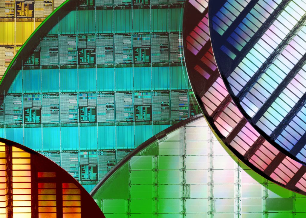
Semiconductor devices include transistors, MEMS, memory (DRAM, flash memory), wafer level packaging (WLP), interconnects and patterning. These devices are manufactured using a variety of process steps, many of which require either high vacuum or low temperature, both core competences of the SHI Cryogenics Group.
Consumer applications of semiconductor technology include:
- Smart phones and tablets (including the accelerometers and gyroscopes built within)
- Televisions, Blu-ray players and video game consoles
- Computers, memory cards and USB flash drives
- Automobile navigation and airbag sensors, medical and communications devices, industrial robotics and many more
Molecular Beam Epitaxy
Molecular Beam Epitaxy (MBE) is an advanced thin-film deposition system widely used in the manufacture of semiconductor devices. With the help of SHI cryopumps, ultra-high vacuum chambers create a clean, dust-free environment for the growth of crystals used in this process.
Chemical Vapor Deposition (CVD)
In this coating process, a substrate (usually a wafer) is exposed to a gaseous mixture, producing a thin film layer. Since many semiconductor manufacturing processes utilize CVD, most modern electronics would not exist without this technology.
Ion Implantation
Ion implantation is a low-temperature surface treatment process essential to manufacturing semiconductor wafers and other integrated circuits. During this process, an ion beam penetrates the surface of a wafer, injecting critical dopants, or impurities, that modify its electrical conductivity.
Physical Vapor Deposition (PVD)
Like CVD, PVD is a vacuum-coating process that produces a thin film layer on a wafer or other substrate. Each atom in the layer is deposited by condensation from the vapor phase to the solid phase. Sputtering and evaporation are two of the most common PVD processes performed in semiconductor fabs.
MCZ
Magnetic-field-applied Czochralski (MCZ) is a method used in the manufacture of single crystal silicon for large-scale integration (LSI). Manufacturers of superconducting magnets for MCZ utilize cryocoolers to cool the superconducting magnets, creating a magnetic field that is applied to melted silicon to control the crystal growth. SHI’s 4K Cryocoolers are ideal for MCZ applications, replacing the much more expensive and diminishing commodity of liquid helium.